·
Two
day workshop was organized by the department of
Physics and Electronics on “PCB
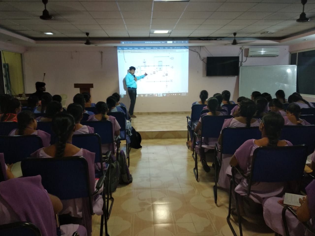
Designing and Manufacturing” in which Mr.V.Govinda
Rao, Director Technical, Microlink, Vijayawada, was the Resource person. In
this technical session 115 students belonging to I B.Sc(MECS),II
B.Sc(MECS),M.Sc Physics have actively
participated and they were divided into 28 batches.
On 30-8-2018 in the morning session Mr.V.Govinda Rao has given basic
knowledge on PCB Circuit Designing and Manufacturing. In the afternoon session the students
are trained, to design the layout of the circuit on PCB board ,using PCB
wizard software.
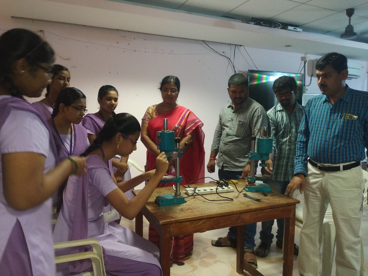
On 31-8-2016, the students have practiced on how to print the design
on PCB circuit board and after that they have done drilling on the circuit
board in order to insert components on the PCB circuit board. At last the
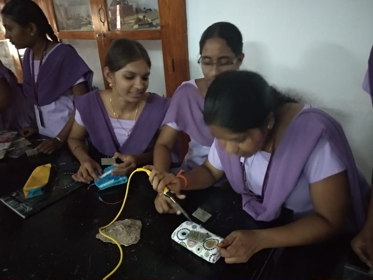
students completed the project by
connecting the components on the board and soldering it. Each student has
done 3 projects namely Regulated
Power Supply , IR tester and Night lamp.
Valedictory session
was held at 3.30 PM in media centre in which the students responded that they
were excited and thrilled to complete three live projects on their own and they
expressed a desire to do more live projects on their own.


No comments:
Post a Comment